IVAM Microtechnology Network
The Fraunhofer Institute for Electronic Nano Systems ENAS is developing a new bonding technology for microsystems in cooperation with Chemnitz University of Technology and SHINKO ELECTRIC INDUSTRIES CO., LTD. The chip-level inductive bonding process was presented for the first time in Tokyo end of January.
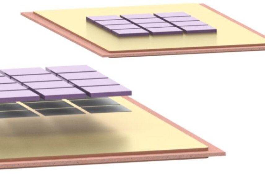
Inductive joining is a technology that has so far mainly been used only for macroscopic components, such as steel tubes or car doors. Fraunhofer ENAS, together with partners, is now developing a process that enables inductive bonding on the micro level for the first time. A bonding process based on sintering paste with silver micro particles was developed for the mechanical surface contacting of chips on DBC (direct bonded copper) substrates.
A wide range of advantages can be exploited here, especially in the heterogenous integration of chips and components. The inductive process enables very rapid heating of targeted structures, for example bond pads, which are joined to the bond partner at a high local temperature. The temperature input occurs primarily locally in the areas of the induction coils, so that the surrounding structures and components, as well as the entire substrate, are significantly less thermally affected by the very rapid heating and cooling of the local structures.
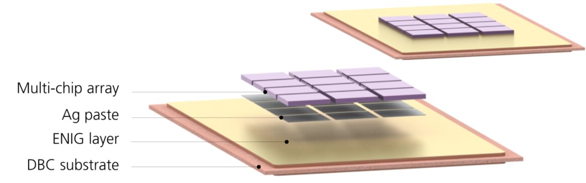
Bonding processes of silicon chips on a DBC substrate have already been successfully carried out with silver sintering pastes. Using induction coils, geometrically adapted to the bond structures, a high-frequency electromagnetic field induces eddy currents in the electrically conductive silver particle pad. Heating rates of more than 100 K/s were thus generated. The overall process time is decisively reduced with this method, since the target temperature of 300 °C is reached in only five seconds.
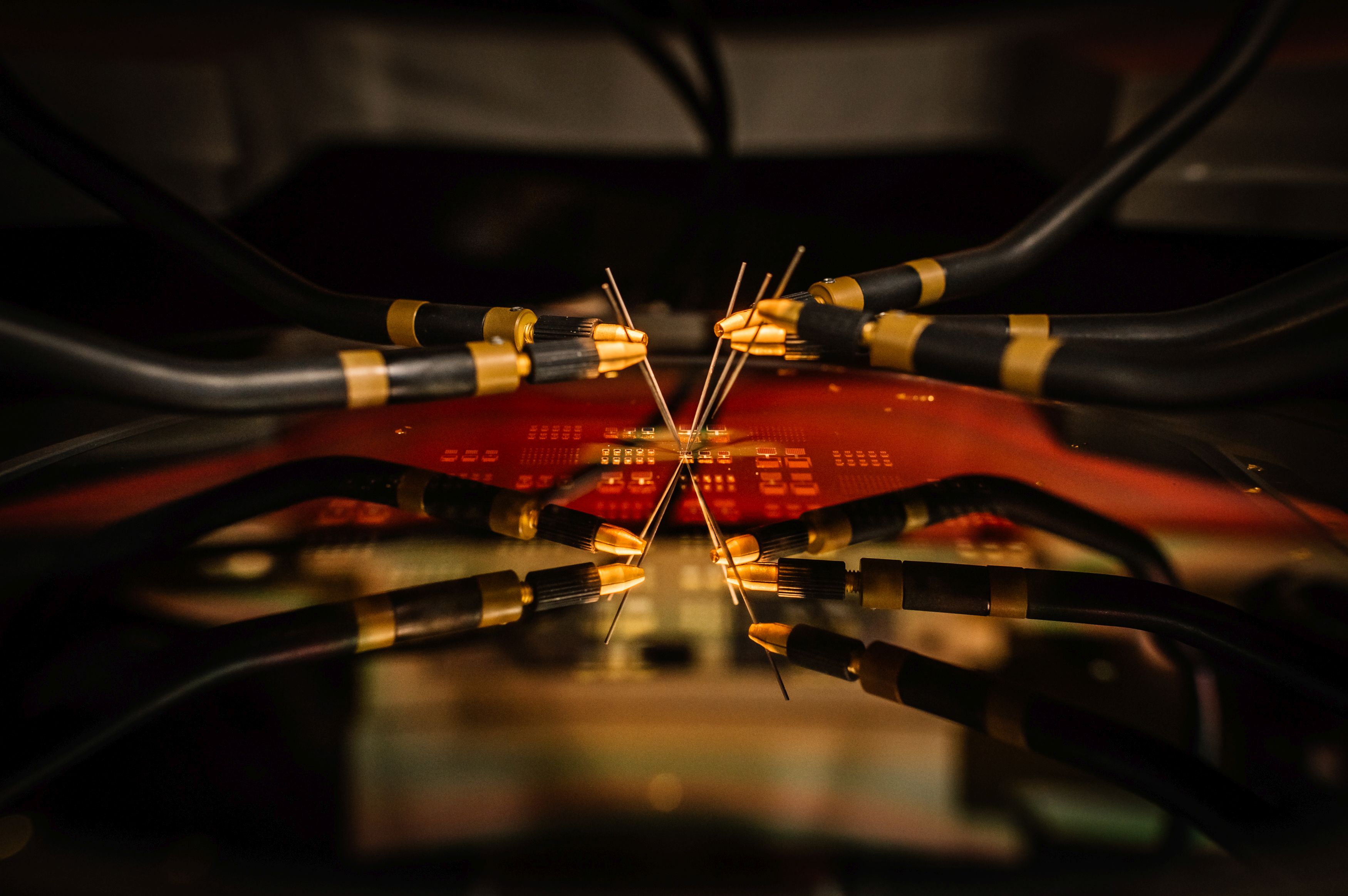
As part of the research work, a test setup consisting of a process chamber with a sintering module, a pressure plate and an infrared camera for process monitoring was developed. The sintering module contains a water-cooled induction coil in an electrically insulating surrounding material. By means of process monitoring, the coil current and the operating frequency are recorded in real time.
This process is revolutionary, especially for manufacturers of power electronics assemblies, as the duration of bonding processes is significantly reduced and the thermal influence on all bonding components is reduced. The mechanical contacting by silver sintering pastes allows the high waste heat of the components to be dissipated quickly and specifically via the sintered structures. The company Shinko offers the process as an industrialized method and is continuously developing the process together with the project partners of Chemnitz University of Technology and Fraunhofer ENAS.
The first Chemnitzer Seminar of the year 2025 is entitled “Test and Reliability Solutions – new opportunities for electronic components …
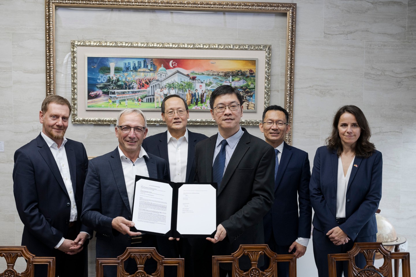
The Fraunhofer Institute for Electronic Nano Systems ENAS in Chemnitz is expanding its strategic collaborations in Southeast Asia. In October …
 AEMtec.jpg)
AEMtec GmbH celebrates 25 years as a leading specialist in micro and optoelectronics. Marking the anniversary, the company is strengthening …
.jpg)
 (1).1.png)