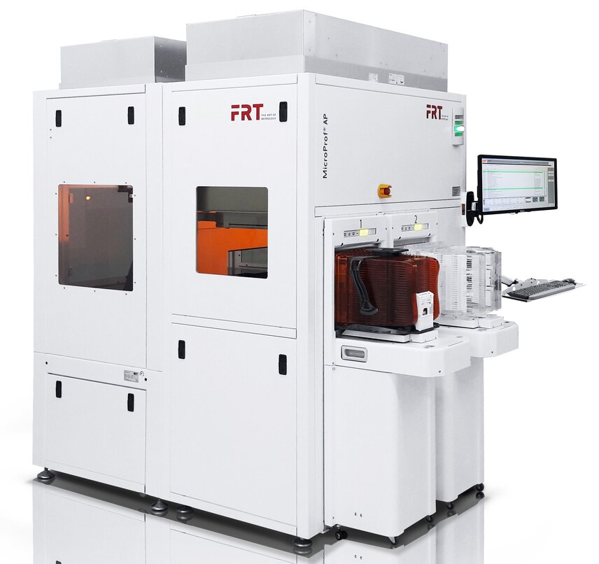
FRT GmbH introduced the MicroProf AP, a metrology tool, especially developed for demanding applications in 3D IC packaging. This is a comprehensive measuring tool with which metrology tasks can be solved throughout the entire process chain and which is able to handle wafers and panels, thinned and bonded wafers, and film frames.
The MicroProf AP is ideally suited to perform measurement tasks of typical process steps in advanced packaging, like photoresist coating and structuring, critical dimension (CD) and overlay measurement, through-silicon vias (TSVs) or trenches after etching, isolation and barrier layer deposition, TSV filling as well as chemical mechanical polishing (CMP). The fabrication of redistribution layers (RDLs), under bump metallization (UBM), BGAs, micro and solder bumps, temporary carrier bonding and debonding, backside thinning, reveal of TSV copper nails, dicing and stacking and measurement of mold- and contact pad surfaces are among the typical tasks.
The modular multi-sensor concept enables this universal metrology tool to flexibly perform various measurement tasks in backside processing (backgrinding, metallization) for power semiconductors such as MOSFET or IGBT, as well as for the control of different substrates, e.g. bulk Si, SOI, cavity SOI, compounds such as GaAs, InP, SiC, GaN, ZnO and also for transparent materials.
Furthermore it can be used for hybrid bonding and Micro Electro Mechanical Systems (MEMS), included in consumer electronics, automotive, telecom, medical and industrial markets. MEMS are manufactured in processes similar to semiconductor production. The MicroProf 300 multi-sensor metrology tool is used for the metrology part. It allows both, the measurement of wafers at different process steps and to enhance the precision of measurements. Using a hybrid metrology concept means integrating information from different sensors and measuring principles in one automated recipe to create new data that previously could not be measured.
The measurement system is equipped with a granite base setup, with a three point sample fixture or a vacuum chuck. Besides the standard configuration, the tool can be equipped with numerous additional features, which can also be retrofit at a later time. With a wafer handling system within an Equipment Front End Module (EFEM) and almost maintenance free hardware components, the product provides high throughput and is the perfect workhorse in any HVM 3D IC fab.
Contact: Sarah Trompetter, FRT GmbH
trompetter@frt-gmbh.com


.png)