IVAM Microtechnology Network
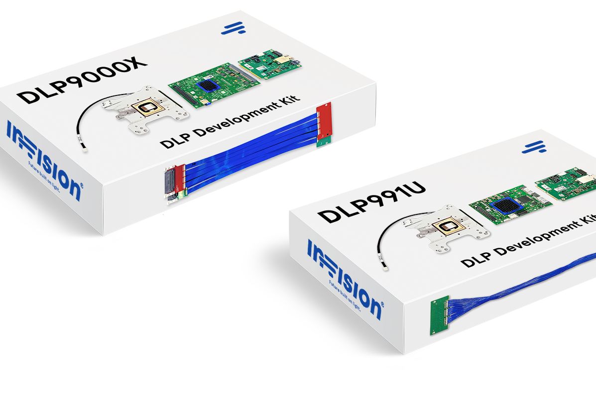
IN-VISION Technologies AG, an Austrian optics company and official Texas Instruments Design House Partner, is expanding access to its advanced …
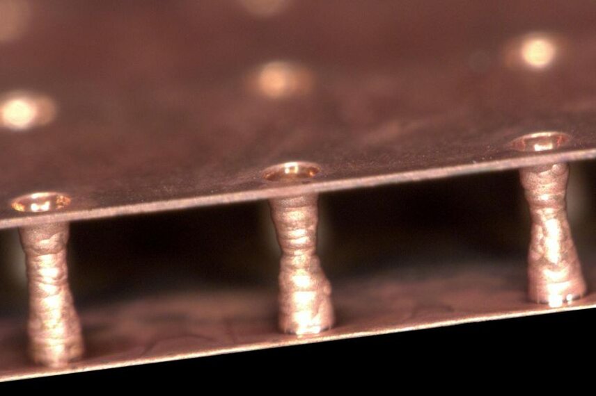
The optical industry almost completely relies on mechanical processes in its process chains. This, however, could soon change. The Fraunhofer …
.png)
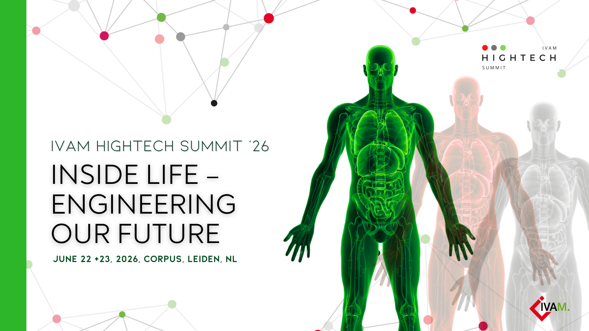
On 22–23 June 2026, the IVAM Hightech Summit will take place in Leiden, the Netherlands. Hosted at CORPUS, the 1.5-day …
).1.png)