FRT GmbH introduced the MicroProf AP to the market. The fully automated metrology tool is specially developed for demanding applications in 3D IC packaging. With the MicroProf AP, FRT offers a comprehensive measuring tool with which metrology tasks can be solved throughout the entire process chain and which is able to handle wafers and panels, thinned and bonded wafers, and film frames.
Suited for typical process steps in advanced packaging
The MicroProf AP is ideally suited to perform measurement tasks of typical process steps in advanced packaging, like photoresist coating and structuring, critical dimension and overlay measurement, through-silicon vias (TSVs) or trenches after etching, isolation and barrier layer deposition, TSV filling, chemical mechanical polishing, fabrication of redistribution layers (RDLs), under bump metallization (UBM), BGAs, micro and solder bumps, temporary carrier bonding and debonding, backside thinning, reveal of TSV copper nails, dicing and stacking and measurement of mold- and contact pad surfaces.
Furthermore, it can be used for hybrid bonding and MEMS, included in consumer electronics, automotive, telecom, medical and industrial markets. With a wafer handling system within an equipment front end module, the MicroProf AP provides high throughput and is the perfect metrology tool in any HVM 3D IC fab.
Contact: Sarah Trompetter, FRT GmbH
trompetter@frt-gmbh.com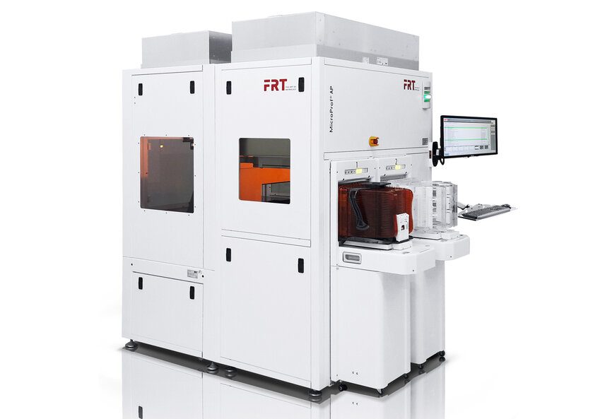

.jpg)